In the article “BCD to 7 Segment Display Driver” you will learn about 7 segment display driver IC SN74143, its key parameter and its application.
Description of BCD to 7 Segment Display Driver | SN74143
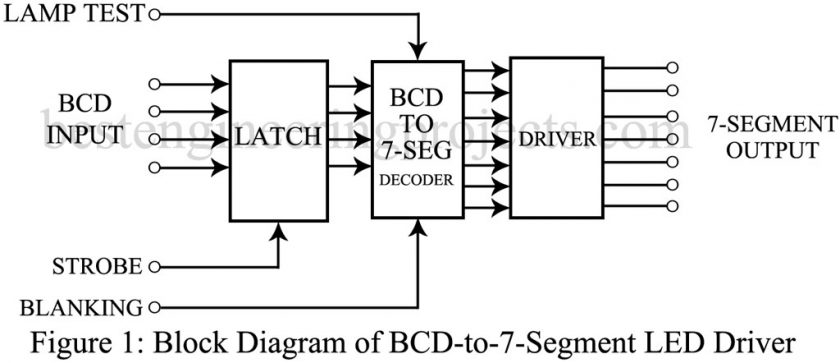
The universal use of 7-segment numerical displays has resulted in a wide range of ICs capable of driving them. One of the most widely used is illustrated in the block diagram of figure 1. The BCG input is applied to a set of four flip-flops which are used as a “latch.” The “strobe” signal determines when the information presented at the input is stored in the latch and when it is erased. The BCD-to-7-segment decoder is effectively the same as described in previous article “BCD to 7 segment decoder” and there are seven separate driver stages.
As illustrated in figure 1, a lamp test and a blanking signal are applied to the decoder portion. The purpose of the lamp test signal is to illuminate all seven sections of the numerical display, and the blanking signal can be used to turn off the entire display for zero blanking multidigit displays, or else to control the on-off time when a series of displays operates in a power conserving, multiplexed mode.
The voltage and current capability of the driver stage determines which type of 7-segmnet numerical displays can be driven. A typical high-voltage CMOS IC can operate up to a maximum of 20 V and can source up to 25 mA at each output. This makes it possible to drive LED displays, low-voltage fluorescent displays, and even incandescent displays. To drive liquid crystal display (LCDs), some other characteristics are necessary which are provided in the IC described in article “”.
Key Parameter of BCD to 7 Segment Display Driver | SN74143
The electrical characteristics are essentially the same as those of the particular digital IC family.
- Maximum power dissipation: 500 mW for a high-voltage CMOS IC. 250 mW for TTL ICs.
- Quiescent current: The maximum current drawn when the IC is not operating. 100 mA at 20 V supply and +250 is typical for high-voltage CMOS.
- Propagation delay time: The time required between data input and output. A maximum of 1,000 ns is typical for high-voltage CMOS devices at 5V power supply.
- Minimum setup time: The minimum time required from the data input until it is stored in the latches. 150 ns is typical for high-voltage CMOS ICs.
- Strobe pulse width: The minimum width of the strobe signal controlling the storage of the data. 400 ns for high-voltage CMOS at 5V supply.
- Output circuit: the method of driving the different types of displays determines what type of output circuit should be used. Many high-voltage CMOS devices use an open-collector-emitter circuit, and this requires separate series resistors for each output when driving and LED. Low-voltage fluorescent displays can be driven directly, but incandescent displays require a small pull-up resistor for each output to the power supply voltage.
Applications
This IC is used to drive common-cathode LED displays either as single units, or as multiplexed series of displays. Incandescent and low-voltage fluorescent displays can also be driven with this IC.
Representative Part Number: Texas Instruments SN74143
