What is Volt Ampere Characteristic of PN Diode?
Current I in a PN diode in related to the junction voltage VV by the relation given by equation,
………..(1)
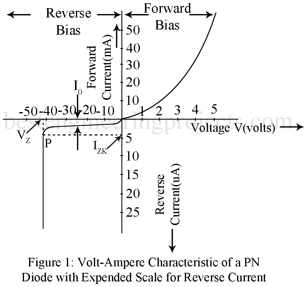
Figure 1 gives the typical volt-ampere characteristic for a PN diode plotting above equation. With forward bias, the forward current remains essentially zero until the so called Cutin voltage VV of t diode is reached. This cutin voltage is defined as the voltage below which the forward current is less than 1% of the maximum rated current of the diode. This cutin voltage is also known as the turn-on voltage or threshold voltage. The cutin voltage varies with the semiconductor material and with the method of fabrication. Typically, the cutin voltage is about 0.2 volt for Ge diode and about 0.6 volt for Si diode. This higher value of cutin voltage in Si diode results mainly due to low value of IO.
From figure 1 we observe that beyond the cutin voltage, the forward current increases rapidly with the increase of forward voltage. In the range of forward voltage, the applied voltage is much larger than VT (0.026 volt at 300 K) so that in above equation we may neglect 1 in comparison with and reduced to the following simpler form
………(2)
With small reverse bias, the reverse current increases with increases with increase in the magnitude of reverse bias. When the reverse bias magnitude exceeds several times VT, we may neglect is comparison with I and the reverse current becomes steady at value IO. with further increase of reverse voltage, the breakdown takes place and the reverse current then increases abruptly at an almost constant value of reverse voltage VZ.
Temperature Dependent of Volt Ampere Characteristic
Total Reverse Saturation Current:
Total or measured value of reverse saturation current where I0 is the theoretical value of reverse saturation current and IR is the leakage reverse current component. IR is independent of temperature whereas I0 is heavily dependent on temperature.
…….(3)
This equation gives I0 as a function of Dn, Dp and ni2. But ni2 depends on temperature as given by equation below
……..(4)
Voltage VT is also proportional to temperature T. Further Dp and Dn depend on temperature T. Accordingly a general expression for I0 valid for both Ge and Si diodes is,
……….(5)
Where k is a constant, m is a constant for the material, qVG0 is the forbidden energy gap in joules. Experimentally it is found that reverse saturation current increases at the rate of 7% per deg C for both Ge and Si diodes. But
. Hence, we conclude that the total reverse saturation current doubles for every 100 C rise in temperature.
Cutin Voltage:
The following relation is found valid for both Ge and Si diodes,
……..(6)
Thus, V and also VV decrease with the increase of temperature at the rate of 2.5 mV/deg C. Although the cutin voltage VV and total reverse saturation current change with temperature, the shape of the overall V-I characteristic of diode does not change with temperature.
Diode resistance:
Static Diode Resistance R
It is the ratio of diode voltage to diode current. It varies greatly as the operation point shifts. It does not form a useful parameter of diode.
Dynamic or Incremental Diode Resistance r
It is defined as,
……….(7)
Thus, dynamic resistance of a diode is the reciprocal of the slope of current versus voltage characteristic and forms an important device parameter for small signal operation. However, the dynamic diode resistance r varies with the operation point.
From, equation (1),
……..(8)
For reverse bias greater than a few tenth of a volt, and negative. Hence,
is extremely small composed to unity and hence r is extremely large.
For forward bias greater than a few tenth of a volt,
and as per equation (1), I>>I0. Then from Equation (8).
………(9)
Equation (9) shows that for forward bias, r various inversely with the current I.
At room temperature (300 K), VT = 0.026 volt. Then for ,
…….(10)
Thus, for
Example 1: An ideal Ge diode operating at temperature of 1000C, has reverse saturation current . At 1000C, find the dynamic resistance of the diode for a bias of 0.1 volt (a) in the forward direction and (b) in the reverse direction.
Solution:
At 1000C, T = 273 + 100 = 3730K,
Hence,
For Ge,
Hence,
Now,
For forward bias of 0.1 volt,
Hence,
For reverse bias of 0.1 volt,
Hence,
Piecewise Linear Approximation of Diode Characteristic
For large single operation, it is usually sufficient to use a piecewise linear representation of the V-I characteristic of PN diode. Figure 2 shows a piecewise linear approximation. For V < VV the current rises with a constant slope. In this region, the diode has a constant incremental resistance . In this forward bias region, this resistance r is designated as Rf and is called the forward resistance.

