A bipolar junction transistor (BJT) forms an extension of a PN diode. It is three-layer semiconductor device with two junctions. Further it is a bipolar device i.e. the current is carried by two types of charge carriers namely electrons and holes and hence the device is called a Bipolar Junction Transistors. A BJT is basically used as an amplifier i.e. as a circuit for amplifying or increasing the magnitude of a periodic or an a-periodic voltage or current.
A junction transistor may be of PNP type or NPN type and may be made of germanium or silicon. A PNP transistor consists of a crystal of silicon (or germanium) in which a thin layer of n-type silicon is sandwiched between two layers of p-type silicon. An NPN transistor, on the other hand, consists of a silicon (or germanium) crystal in which a thin layer of p-type silicon is sandwiched between two layers of n-type silicon.
Types of Transistor on the Method of Construction
Type of Transistors: Depending on the method of construction transistors may be classified in following five categories:
- Grown Junction Transistors
- Alloy type of Fused Junction Transistors
- Diffused Junction Transistors
- Epitaxial Planar Transistors
- Transistors
Grown Junction Transistor | Types of Transistor on the Method of Construction
Figure 1 and 2 show respectively the three- and two-dimensional views of basic grown junction PNP transistor. Such a transistor is formed by first growing a Ge (or Si) crystal of p-type from a melt of Ge (or Si). Later on, the type of impurity is changed to n-type by adding to the melt, n-type impurity in sufficient large quantity and after a very small-time interval, again the impurity is changed to p-type by adding sufficient p-type impurity. Thus, there get formed a very thin layer of n-type semiconductor sandwiched between p-type materials on either side. The thin central section is called the base whereas and end sections constitute the emitter and the collector. The base region is extremely thin, or less. Two junctions are formed: the emitter-to-base junction or simply the emitter junction JE and Collector-to-base junction or simply the collector junction JC.


The continuously large crystal formed from the melt is cut into a large number of small thin constant width slices by cutting along the planes at right angles to the planes of junctions. Next each slice is cut normal to the slice surface thereby resulting in a number of semiconductor bars of rectangular sections. Each such bar contains all the three regions and the two junctions and ultimately forms a grown junction transistor. Each bar is polished and etched. Non-rectifying electrodes are deposited at each end of the bar and wires or leads are attached to the end electrodes to form the emitter and the collector leads. Similarly, leads are attached to the thin base reign. The whole assembly is then etched and covered with moisture proof grease, mounted in a suitable mechanical structure and then hermetically sealed within a small glass envelope with leads passing through the foot. Opaque paint is usually coated on the outside of glass envelope to exclude incident light.
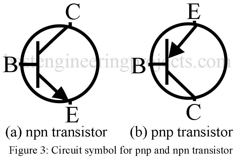
Figure 3 shows the circuit symbols for PNP and NPN transistors applicable to all types of transistors irrespective of the method of construction. The thick horizontal line represents the base while the two inclined lines represent the emitter and the collector. The emitter is identified by an arrow head placed on the inclined line. The direction of the arrow head gives the direction of the conventional electric current with emitter given forward bias. Thus, in a PNP transistor, holes flow from emitter into the base region. The direction of the conventional electric current is also from emitter into the base. Hence, in the symbol for PNP transistor, arrowhead on the emitter electrode points into the base as shown in figure 3 (a). In an NPN transistor, on the other hand, electron flow from emitter into the base and the conventional electric current flows from base into the emitter. Hence, in the symbol for NPN transistor, arrowhead on the emitter electrode points away from the base as shown in figure 3(b). Sometimes letter E, B and C are added as shown in figure 15 to designate emitter, base and collector respectively. Further sometimes the entire symbol is enclosed within a circle as shown.
Alloy Type (or Fused Junction) Transistor | Types of Transistor on the Method of Construction
Figure 4 gives the structure of a PNP fused junction transistor. It basically consists of a thin small wafer of Ge (or Si), with thin pallets of some p-type dopant typically indium alloyed on either side forming the emitter and collector. The collector pallet is about 3 times larger than the emitter pallet. This assembly is then heated to about 5000C in an atmosphere of hydrogen. At this temperature, indium pallet (melting point 1550 C) melts. However, Ge does not melt since its melting point is above 5000 C. Molten indium dissolves some of the Ge from the wafer and forms a saturated solution. On cooling, solution recrystallizes to form a p-type Ge at the solid liquid interface. On further cooling, the rest of the indium solidifies. Leads are soldered to the indium pallets forming emitter and collector terminals. Contact to the base is made by welding a strip or loop of gold-plated wire to the base plate. The resulting assembly forms a pnp transistor with two junctions on opposite faces of the Ge wafer. The spacing between the junctions inside the base wafer is extremely small, a few mils and this forms the base thickness. This effective base thickness depends on the temperature to which the assembly is heated and on the period of heating.
Complete assembly is then etched to remove surface impurities, covered with moisture proof grease, suitable mounted in a mechanical structure and sealed inside a glass envelop with leads brought out from the bottom. Opaque paint is usually coated on the outer surface of the glass envelope to avoid incident light.
Diffused Junction Transistor | Types of Transistor on the Method of Construction
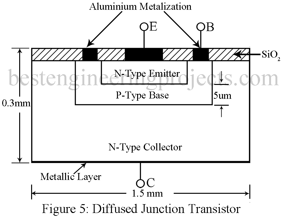
Figure 5 shows the basic structure of a diffused junction transistor. A thin layer of SiO2 is thermally frown own the top surface of a small (1.5 mm x 1.5 mm) silicon chip of thickness typically 0.3 mm. The SiO2layer is photo-etched to form a mask and p-type diffusion is permitted through the opening in the SiO2 mask. For this diffusion process, the Si wafer is placed in a furnace at 10000C in a gaseous atmosphere of a high boron concentration. A sharp impurity concentration gradient results at the surface of the wafer and hence boron diffuses into the Si wafer.
At this high temperature (10000C), several Si atoms move out of their lattice sites leaving vacancies for impurity boron atoms to move in. Again, a layer of SiO2 is thermally grown at the top and photo-etched. Emitter diffusion (n-type) is made through the opening in SiO2 layer resulting in a small n-type region. The resulting p-type base has very small width of or less. Finally, a fresh layer of SiO2 is thermally grown, photo-etched and aluminum contacts are made through the opening for the emitter and base leads resulting in the structure shown in figure 5. A metallic layer is formed at the bottom of the wafer and collector lead is attached to it.
Epitaxial Planner Transistor | Types of Transistor on the Method of Construction
Figure 6 shows the basic structure. Here a very thin high purity single crystal layer of typically n-type Si is grown on the heavily doped substrate of the same material. This complete structure then forms the n-type collector on which p-type base and n-type emitter regions are diffused in sequence. Use of thin epitaxial high resistance collector layer results in (i) increased breakdown voltage and hence increased working voltage and (ii) reduced base current. Further reduces base and emitter areas result in higher upper frequency limit and improved switching time.
Misc. Transistors | Types of Transistor on the Method of Construction
In some cases, the above-mentioned techniques may be combined. Thus, we may have transistors of the following types: (i) diffused allow type (ii) grown-diffused type (iii) allow emitter-epitaxial base type etc.
It is of interest to note that the earliest transistors that were developed, were the point, contact transistors. A point contact transistor consists of two sharply pointed tungsten wires pressing against a semiconductor wafer. Such transistors suffer from poor reliability and reproductively. Hence, such transistors are no longer commercially used.


