Three are two types of electrical/electronics appliances based on the main supply it requires. Generally, heavy electrical equipment requires a three-phase main supply for working. Three-phase mains supply has three different phases each are placed at 1200 angle with each other. In this post, you will learn how to design a three-phase power surge protector circuit using timer IC 555. A three-phase electrical appliance is expensive and requires all phase supplies, if voltage fluctuates or fails in any phase operation of the appliance may malfunction or become dead. In order to solve this problem, we are designing this appliance protector circuit.
Operation of Power Surge Protector Circuit:
If the voltage at any phase fails, this circuit switches off the appliance and resume automatically when the voltage at all phase is available with a certain delay. This delay protects the appliance from surge and hence eliminate fluctuations.
Component required of power surge protector circuit
| Resistor (all ¼-watt, ± 5% Carbon Unless Stated Otherwise) |
| R1 – R3 = 3.3 KΩ
R4 = 4.7 KΩ VR1 = 1 MΩ |
| Capacitors |
| C1 – C3 = 100 µF, 35V (Electrolytic capacitors)
C4 = 4.7 µF, 35V (Electrolytic capacitors) C5 = 0.01 µF (Ceramic Disc) |
| Semiconductors |
| IC1 = NE555 (Timer IC)
T1 = SL100 (Medium power NPN Transistor) D1 – D6 = 1N4001 (Rectifier Diode) LED1 = 5mm Red Color LED LED2 = 5mm Yellow Color LED LED3 = 5mm Blue Color LED |
| Miscellaneous |
| RL1 – RL4 = 12V, 1CO Relay
RL4 = 230V Coil rating contactor, 4 contact current rating 32A. X1 – X3 = 230V AC Primary to 0-12V 300mA Secondary Transformer |
Circuit Description of Three-Phase Power Surge Protector Circuit
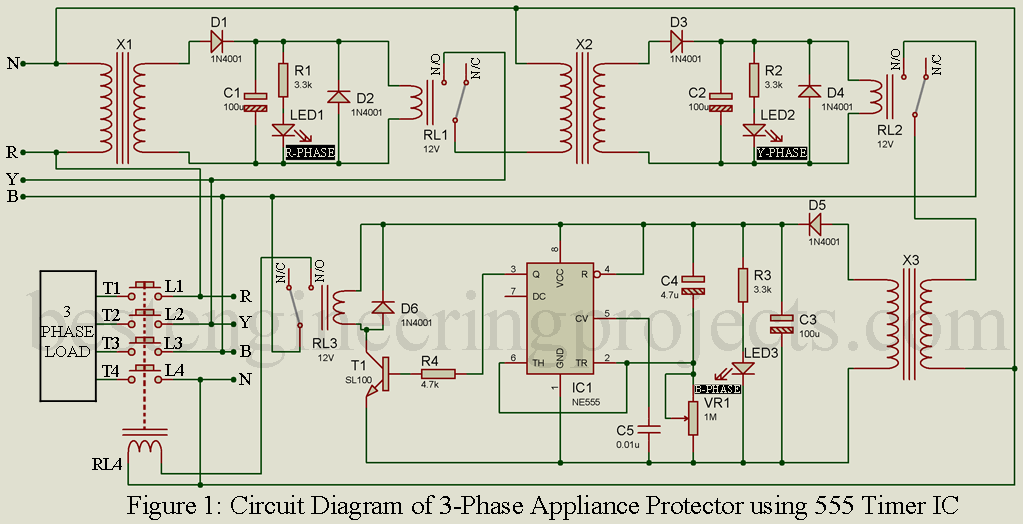
The circuit diagram of the appliance protector is shown in figure 1, build around timer IC 555, relay, transformer, and a few other passive and active electronic components. This circuit utilizes three transformers and three relays one for each phase. One terminal of each primary winding of the transformer is connected to neutral mains supply whereas another terminal of each transformer is connected to each phase of the mains line i.e. R, Y, and B phase respectively as shown in the circuit diagram. Relay RL1 and RL2 are configured in such a way that its output behaves as AND gate i.e. its output is high only when all the input is high and becomes low in all other cases.
Let’s see the operation of the circuit. R-phase is connected to one terminal of transformer X1 when neutral is connected to another terminal. When R-phase is available then secondary winding of transformer X1 and stepdown voltage is available which is rectified by half-wave rectifier designed using diode D1 and filtered using capacitor C1. This voltage energized the relay RL1 and hence its common pin contact with Normally-Opened (N/O) contact. The N/O contact of the relay is connected to the Y-phase of the mains line and the common pin of the relay is connected to one terminal of the primary winding of transformer X2 where another terminal is connected to the neutral line as shown in the circuit diagram. The rest of the process is the same as previously described.
The basic function is to rectify the step-down voltage and energize the relay RL2. Thus, from the above description, we can say that relay RL2 is only energized when both the R-phase and Y-phase are available. When relay RL2 is energized the common pin connects to the N/O pin of relay RL2. The N/O pin of the relay is connected to the B-phase of the mains line and the common pin of relay RL2 is connected to one terminal of the primary winding of transformer X3 where another terminal of the primary winding is connected to the neutral line.
Voltage is available to the primary winding of transformer X3 only when all the three phases (R, Y, and B phase) are available. When all the phase is available, step-down voltage is available at the secondary winding of transformer X3 which is rectified and filtered by diode D5 and capacitor C3 respectively. This voltage activates the time delay circuit.
The time delay circuit is designed around timer IC 555, configured in monostable mode. When all the phase is available timer IC 555 get triggered and activate the output. For the given configuration the time delay should be 4 seconds.
The mathematical calculation involved in the time delay circuit
Charge capacitor C4 = 4.7 µF
Resistor = 1 MΩ Variable
Time Delay = 4 Sec.
Now, lets find the value of resistor for 4 second time delay
T = 1.1RC
Or, 4 = 1.1 x R x 4.7×10⁻⁶
R = 773KΩ
Therefore, at about ¾ position of the wiper of variable resistor VR1, the output delay will be 4 sec. But you can change this delay according to your requirement by adjusting the wiper of the variable resistor.
When all the phase is available the relay RL3 is energized and it activates the contractor and hence appliance gets all the three-phase supply.
Glowing LED1 (Red LED) ensures the availability of the R-phase whereas LED2 and LED3 ensure the Y and B phase of the mains line.
Note: The rating of the contractor must be according to the load you operate.