In the topic “Noise Designation and Calculation” we will discuss the various topics with proper mathematical equations and examples. The topic we are going to discuss are:
- Signal to noise ratio
- Noise Figure
- Resistor combination effect
- Reactance Noise effect
- Noise due to amplifier in a cascade
- Equivalent noise temperature
- Equivalent noise resistance
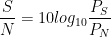
Signal-to-Noise Ratio
We have thus far dealt with different types of electrical noise without showing how to deal with noise in a practical way. The most fundamental relationship used is known as the signal-to-noise ratio (S/N ratio), which is a relative measure of the desired signal power to the noise power. The S/N ratio is often designated simply as S/N and can be expressed mathematically as
 ….(1)
….(1)
at any particular point in an amplifier. It is often expressed in decibel form as
 …(2)
…(2)
For example, the output of the amplifier in Ex. 1-2 was 1 mV rms and the noise 0.514 mV rms, and thus (remembering that  )
)
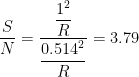 or
or 
Noise Figure
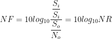
S/N very well identifies the noise content at a specific point but is not useful in relating how much additional noise a particular transistor has injected into a signal going from input to output. The term noise figure (NF) is usually used to specify exactly how noisy a device is. It is defined as follows:
 ….(3)
….(3)
where  is the signal-to-noise power ratio at the device’s input and
  , is the signal-to-noise power ratio at its output. The term
  is called the noise ratio (NR). If the device under consideration were ideal (injected no additional noise), then and would be equal, the NR would equal 1, and NF = 10 log 1 = 10 x 0 = 0 dB. Of course, this result cannot be obtained in practice.
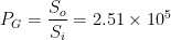
Example 1: A transistor amplifier has a measured S/N power of 10 at its input and 5 at its output.
(a) Calculate the NR.
(b) Calculate the NF.
(c) Using the results of part (a), verify that Eq. (3) can be rewritten
mathematically as

Solution:
(a) 
(b) 


(c) 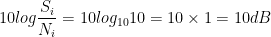

Their difference (10dB – 7dB) is equal to the result of 3dB determined in part (b).
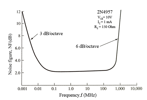
Figure 1: noise figure versus frequency for a 2N4957 transistor
The result of Ex. 1 is a typical transistor NF. However, for low-noise requirements devices with NFs down to less than 1 dB are available at a price premium. The graph in Fig. 1 shows the manufacturer’s NF versus frequency characteristics for the 2N4957 transistor. As can be seen, the curve is flat in the mid-frequency range ( ) and has a slope of -3 dB/octave at low frequencies (excess noise) and 6 dB/octave in the high-frequency area (transit-time noise). An octave is a range of frequencies in which the upper frequency is double the lower frequency.
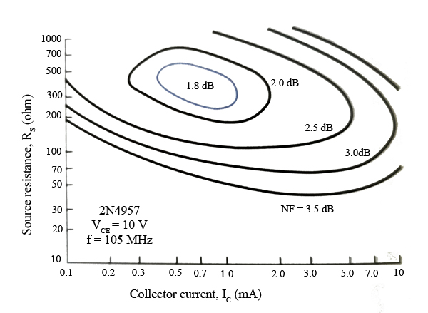
Figure 2: Noise Contours for a 2N4957 Transistor
Manufacturers of low-noise devices usually supply a whole host of curves to exhibit their noise characteristics under as many varied conditions as possible. One of the more interesting curves provided for the 2N4957 transistor is shown in Fig. 2. It provides a visualization of contours of NF versus source resistance and dc collector current for a 2N4957 transistor at 105 MHz. It indicates that noise operation at 105 MHz will be optimum when a dc (bias) collector current of about 0.7 mA and source resistance of 350 ohms is utilized since the lowest NF of 1.8 dB occurs under these conditions.
The current state of the art for low-noise transistors offers some surprisingly low numbers. The leading edge for room temperature designs at 4 GHz is an NF of about 0.5 dB using gallium arsenide (GaAs) FETs. At 144 MHz, amplifiers with NFs down to 0.3 dB are being employed. The ultimate low-noise-amplifier (LNA) design utilizes cryogenically cooled circuits (using liquid helium). Noise figures down to about 0.2 dB at microwave frequencies up to about 10 GHz are thereby made possible.
Resistor Combinations effect
The noise effect of more than one resistor can be determined by the concept of equivalent resistance. This is clearly shown by the following example.
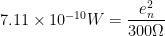
Example 2: Two resistors, 5 K-ohm and 20 K-ohm are at 27°C. Calculate the thermal noise power and voltage for a 10-kHz bandwidth
(a) For each resistor.
(b) For their series combination.
(c) For their parallel combination.
Solution


Note that this is the noise power for all resistor values/combinations.

Reactance Noise Effects
In theory, a reactance does not introduce noise to a system. This is true for ideal capacitors and inductors that contain no resistive component. The ideal cannot be attained, but fortunately, their resistive elements usually have a negligible effect on system noise considerations compared to semiconductors and other resistances.
The significant effect of reactive circuits on noise is their limitation on frequency response. Our previous discussions on noise have assumed an ideal bandwidth that is rectangular in response. Thus, the 10-kHz bandwidth of Ex. 1-5 implied a total passage within the 10-kHz range and zero effect outside. In practice, RC-, LC-, and RLC-generated passbands are not rectangular but slope off gradually, with the bandwidth defined as a function of half-power frequencies. The equivalent bandwidth  to be used in noise calculations with reactive circuits is given by
 ….(5)
….(5)
where BW is the 3-dB bandwidth for RC, LC, or RLC circuits. The fact that the “noise” bandwidth is greater than the “3-dB” bandwidth is not surprising. Significant noise is still being passed through a system beyond the 3-dB cutoff frequency.
Noise Due to Amplifiers in Cascade
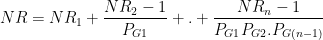
We previously specified that the first stage of a system is dominant concerning the noise effect. We are now going to show that effect numerically. Friiss’ formula is used to provide the overall noise effect of a multistage system.
 …..(6)
Where NR = overall noise ratio of n stages
 = power gain ratio
Example 3: A three-stage amplifier system has a 3-dB bandwidth of 200 kHz determined by an LC tuned circuit at its input, and operates at 22°C. The first stage has a power gain of 14 dB and an NF of 3 dB. The second and third stages are identical, with power gains of 20 dB and NF = 8 dB. The output load is 300 ohm. The input noise is generated by a 10 k-ohm resistor. Calculate
(a) The noise voltage and power at the input and the output of this system assuming ideal noiseless amplifiers.
(b) The overall noise figure for the system.
(c) The actual output noise voltage and power.
Solution
(a) The effective noise bandwidth is

Thus, at the input,

and


The total power gain is 14 dB + 20 dB + 20 dB = 54 dB.
Therefore,

Assuming perfect noiseless amplifiers,


Remembering that the output is driven into a 300-ohm load and 
we have

Notice that the noise has gone from microvolts to millivolts without considering the noise injected by each amplifier stage.
(b) Recall that to use Friiss’ formula, ratios and not decibels must be used.
Thus,


Thus, the overall noise ratio (2.212) converts into an overall noise figure of 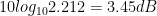 :
:


Therefore,


To get the output noise voltage, since ,

Notice that the actual noise voltage (0.462 mV) is about 50% greater than the noise voltage when we did not consider the noise effects of the amplifier stages (0.311 mV).
Equivalent Noise Temperature
Another way of representing noise is by equivalent noise temperature. It is a convenient means of handling noise calculations involved with microwave receivers (1 GHz and above) and their associated antenna system, especially space communication systems. It allows easy calculation of noise power at the receiver using Eq. (1) since the equivalent noise temperature ( ) of microwave antennas and their coupling networks are then simply additive.
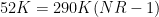
The of a receiver is related to its noise ratio, NR, by
 ……(7)
……(7)
where  , a reference temperature in kelvin. The use of noise temperature is convenient since microwave antenna and receiver manufacturers usually provide information for their equipment. Additionally, for low noise levels, noise temperature shows a greater variety of noise changes than does NF, making the difference easier to comprehend. For example, an NF of 1 dB corresponds to a of 75 K, while 1.6 dB corresponds to 129 K. Verify these comparisons using Eq. (7), remembering first to convert NF to NR. Keep in mind that noise temperature is not an actual temperature but is employed because of its convenience.
Example 4: A satellite receiving system includes a dish antenna ( ) connected via a coupling network (
 ) to a microwave receiver (
 referred to its input). What is the noise power to the receiver’s input over a 1-MHz frequency range? Determine the receiver’s NF.
Solution:


Therefore, 
Equivalent Noise Resistance
Manufacturers sometimes represent the noise generated by a device with a fictitious resistance termed the equivalent noise resistance  . It is the resistance that generates the same amount of noise predicted by
  as the device does. The device (or complete amplifier) is then assumed to be noiseless in making subsequent noise calculations. The latest trends in noise analysis have shifted away from the use of equivalent noise resistance in favor of using the noise figure or noise temperatures.