The demand for high-density, cost-effective printed circuit boards has promoted the electronic industry to seek alternative methods to traditional plated-through-hole technology. One such alternative is surface mounting, a technology traditionally used in hybrid fabrication. The advantage of surface mounting is numerous but the button line is that it is cost effective and will begin to displace plated-through-hole technology as the availability of surface-mount components increases.
Texas Instruments is fully supporting the growth of the surface-mount industry with its line of plastic leaded chip carriers. An introduction to the surface-mount components increases.
Introduction to Surface Mount Technology
The post molded leaded carrier (PLCC) was developed by Texas instruments in 1980 to improve the packing density of ICs on printed circuit (PC) boards and over come some of the size constraints normally caused by duel-in-line (DIP) package. The PLCC was also designed to be used under the same environmental conditions as the DIP without any readability degradation. The PLCC occupies approximately 40% to 60% of the PC board area of an equivalent DIP, and requires no through holes (surface mount), therefore, it lowers the cost on PC boards. Unlike some surface-mounted packages, TI’s PLCC requires no special PV board material considerations. The design of the lead provides compliance allowing the use of any commercial substrate. Digital, Linear, Gate Array, and MOS devices will be offered in 18-, 20-, 28-, 44-, 52-, 68-, and 84-pin packages through TI.
Package Outline
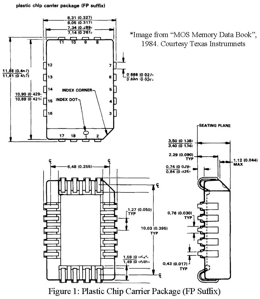
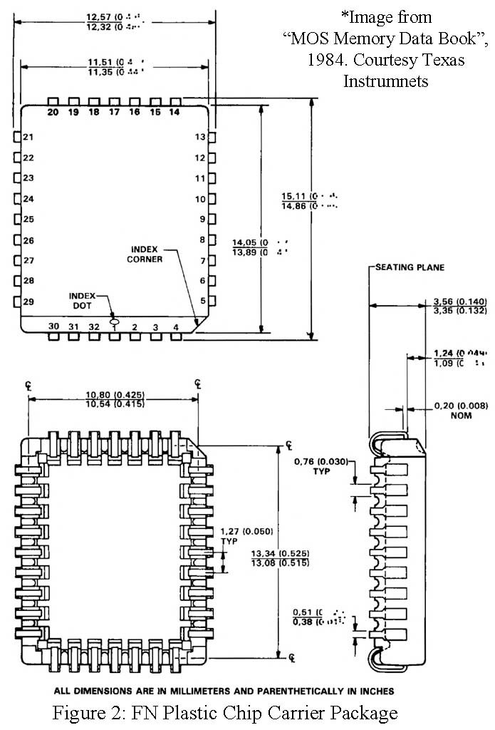
The mechanical data for the PLCCs is given in Figures 1 and 2; their thermal properties are listed in Table 1. The following general statements apply to the packages:
- Each of the chip carrier packages consist of a circuit mounted on the lead frame and encapsulated within an electrically nonconductive plastic compound. The compound withstands soldering temperatures with no deformation, and circuit performance characteristics remain stable when the devices are operated in high humidity conditions.
- These packages are intended for surface mounting on solder pads with 1.27-mm (0.050-inch) centers. The leads require no addition cleaning or processing when used in soldered assembly.
- All dimensions shown are metric units (millimeters), with English units (inches) shown parenthetically. Inch dimensions govern.
- Lead spacing shall be measured within the zones specified.
- Tolerances are noncumulative.
- Lead material CD-155. T60 (Copper Alloy).
- Dimple in top of package denotes pin 1.
| NO. OF LEADS | PACKAGE DESIGNATION | ||
| 18 | FP | 85.4 | 13.8 |
| 20 | FN | 113.6 | 37.1 |
| 28 | FN | 76.8 | 32.2 |
| 44 | FN | 68.0 | 20.3 |
| 68 | FN | 45.7 | 11.4 |
J-Lead Advantage
Texas Instruments PLCC packages are constructed with the J-lead structure due to its superior performance when mounted on a wide spectrum of substrate ranging from ceramic to epoxy-glass. This is possible due to the compliancy of the J-lead which compensates for the possible thermal mismatch between plastic packages and mounting substrates.
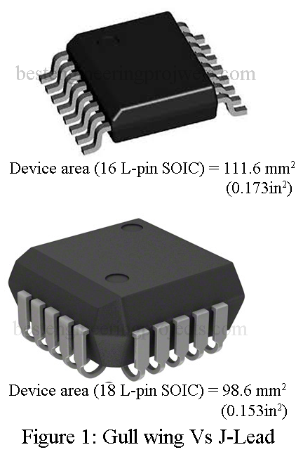
More care must be taken when using ceramic leadless chip carriers mounted on nonceramic substrates in order to prevent solder joint fracturing under thermal cycling. The J-lead also offers advantages over plastic surface-mount packages using different lead structures. Figure 2 gives a comparison of the J-lead used on the PLCC to the “gull wing” commonly used on small-outline integrated circuits (SOICs) and “quad packs”.
Advantages of Gull Wing
- Proven Process
- Positive solder “Witness”
- Easy Auto-positioning
- Nested stacking (Peripheral)
Disadvantage of Gull Wing
- Extends X-Y size
- Leads subject to damage
- High pin count packages impractical
Advantage of J-Lead
- Proven Process
- Leads are complaint, useable with PC board and ceramic substrates.
- Minimum X-Y size, maximum board density
- Easy auto positioning
- Leads well protected.
- Easy Replacement
- Socketing easy
- JEDEC standards exists
- Stand0off from the board allows easy cleaning
- Largest line of available packages: from 18 to 68 leads, Higher pin counts under development
Disadvantage of J-Lead
- Total package hight thicker than SOIC
- Inrfared (IR) Reflow diffiuilt
You may also like:


