In this article we will discuss about buffer or inverter IC, its key parameters, internal circuit and applications.
Description of Buffer or Inverter IC
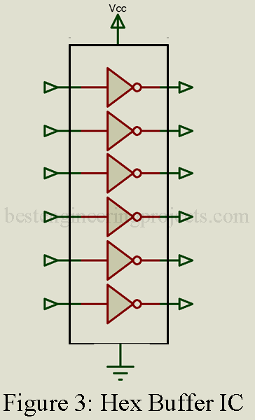
The buffer or inverter is one of the key functions used in all digital logic assemblies. As the name implies, this circuit provides a stage of buffering, separation in impedance, between other logic elements of buffering, separation in impedance, between other logic elements and, when it acts as inverter, changes the input signal into its complement. While buffer or inverters are most frequently used in combination with other key logic elements, they are also available as separate ICs, with six individual stages on a single IC as shown in figure 3.
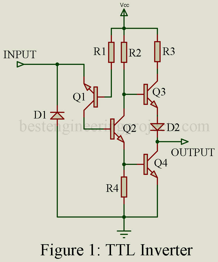
To illustrate the critical function of the buffer inverter, figure 1 includes the actual circuit used to implement a buffer inverter in TTL and CMOS logic. In both circuits the input impedance is higher than the output impedance and the output signal is the inverse, complement, of the input signal.
In the TTL version a buffer or inverter is also available in which R3, Q3 and D2 have been omitted. This allows the user to connect an external collector resistor between the output terminal and Vcc or some other voltage. This “Open Collector” buffer or inverters are particularly useful for level-shifting applications.
Buffer or inverters are available for every logic family and are combined with other circuits to provides special buffering or inverter functions. Some buffers do not invert the input signal; this is indicated by the omission of the circle at the apex of triangular buffer or inverter symbol.
Key parameters
The electrical characteristics are those of the particular digital IC family.
- Input load factor: The number of input loads represented by each buffer or inverter. A typical load factor for TTL and CMOS device is 1.
- Output load factor (fan-out): The number of output loads of the particular digital IC family that the buffer or inverter can drive. A typical TTL buffer or inverter can drive ten TTL inputs. CMOS buffer or inverters can drive a much higher number of CMOS inputs but usually only two TTL loads.
- Propagation delay time: The minimum time a signal is delayed between input and output. For a TTL buffer or inverter 13ns is typical. For a CMOS device 30 to 80 ns is typical.
- Quiescent current: The current drawn by the entire IC when no operations are performed. For TTL devices 2.0mA is typical, while 2.0 nA is typical for CMOS.
Applications
Buffers or inverters are used in all types of digital logic combinations to provide a separation between logic circuits and to increase the fan-out or drive capability of a particular output.
Representative part Number: Texas Instruments 7404.
Checkout the various Digital Electronics Projects.
Comments
The description of a hex buffer or inverter indicated that six identical circuits are contained on one IC. Most manufacturers produce the hex buffer ICs for inverting or noninverting applications. Be sure to check the manufacturers’ identification number to determine which is which.


