FET Parameter
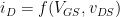
In a FET, instantaneous drain current iD is a function of (i) the instantaneous gate voltage VGS and (ii) instantaneous drain voltage VDS. Thus,
Making use of equation 1, we may define the three FET parameter gm, rd and 
Transconductance gm and Dynamic Drain Resistance rd
Making Taylor series expansion of equation 1 and considering only the first two terms we get,

Using the conventional small signal notation, 


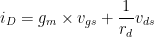
Where,

And,

Parameter gm is called the mutual conductance or the transconductance of the FET and is expressed in mho (or Seimen) or milli-mho (milli-Seimen).
Parameter rd is the dynamic drain resistance of the FET and is expressed in ohms. Drain conductance gd is reciprocal of rd.
Amplification Factor
This is defined as:

By varying vds and vgs is such a way as to keep id = 0, Equation 3 yields:

Or, 
Or, 
All the three parameters gm, rd and
Small Signal Models for FET
Equation 3 gives the incremental drain current id in terms of gm, rd, vgs and vds. Figure 1 gives a circuit which satisfies equation 3 and hence forms the low frequency small signal model of FET. This model contains one dependent current generator whose current gm, vgs is proportional to the time varying gate-to-source voltage vgs. The constant of proportionality is the transconductance gm.

In the low frequency model of FET with gate reverse biased, gate current is zero. Hence, the input resistance between gate and source is infinite. Similarly, the resistance between gate and drain is infinite.
Assuming sinusoidal input voltage of rms value vgs, the model of figure 1 may be redrawn as in figure 2 where vgs, id, vds have been replaced respectively by rms value vgs, Id, and Vds.

Comparison of Low Frequency Model of FET and BJT
Let us compare the low frequency model of FET as given in figure 1 and 2 with the h-parameter model of BJT. We find that
- Both FET and BJT models have a dependent current generator in the output circuit.
- In FET models, the generator current is proportional to the input voltage Vgs whereas in BJT model, the generator current is proportional to the input current.
- In FET, there is no feedback from output (drain) to the input (source) whereas in BJT model, there exists feedback through the parameter hre.
- In FET mode, input resistance is very high, theoretically infinity at low frequencies, whereas in common emitter BJT model, the input resistance is low, being only about 1 k-ohm.
We thus conclude that at low frequencies, FET forms a more ideal amplifier than BJT amplifier.
Magnitude of FET Parameters
Table 1 gives the order of magnitude of the parameters in the low frequency model of diffused junction FET. The table also gives the values of the same parameters for typical low frequency MOSFET.
| Table 1: Values of parameters of Typical JFET and MOSFET | ||
| Parameter | Diffused Junction FET | MOSFET |
| gm
rd rgs rgs |
0.1 to 10 m-mho
0.1 to 1 M-ohm > 100 M-ohm > 10 M-ohm |
0.1 to 20 m-mho
1-50 K-ohm > 104 M-ohm > 106 M-ohm |