Wireless control of devices using infrared is not new to electronics hobbyists. Now, here is wireless control of the device using ultrasonic sound waves tested in BEP Lab. The project ultrasonic Lamp brightness controller circuit uses ultrasonic sound waves (above 20 kHz) for remote control of lamp brightness.
Circuit Description of Ultrasonic Lamp Brightness Controller Circuit
As with all wireless control systems, the Ultrasonic lamp-brightness controller comprises a transmitter and receiver circuit.
Transmitter Circuit | Ultrasonic Lamp Brightness Controller Circuit
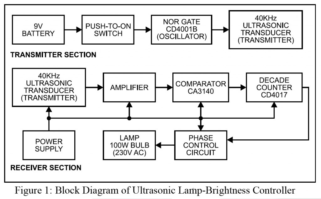
The transmitter circuit generates an ultrasonic sound wave of about 40-50 kHz frequency using an ultrasonic transducer and transmitter circuit. The receiver senses the transmitted frequency from the transmitter circuit, amplifies it, and controls the brightness of the lamp using the corresponding circuit. The block diagram of ultrasonic lamp brightness control is shown in figure 1.
The transmitter section consists, of a decade counter CD4017 (IC1), which is configured as a free-running astable multivibrator. The frequency of 40-50 KHz is generated by the transmitter circuit and is converted into ultrasonic sound waves of the same frequencies by the ultrasonic transducer. The variable resistor VR1 is used for setting the transmitted frequency to 40 kHz.
Receiver Circuit | Ultrasonic Lamp Brightness Controller Circuit
The receiver circuit of the ultrasonic lamp brightness controller is so designed that it receives transmitted ultrasonic sound waves. As in the transmitter circuit, the receiver circuit also used an ultrasonic transducer called the receiver ultrasonic transducer. The frequency received by the receiver is converted into an electrical signal of the same frequencies.
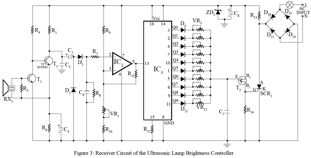
Transistors T1 and T2 are used to amplify the signal up to the appropriate level. The amplified signal is further rectified and filtered by using diodes D1 & D2 and capacitor C6 respectively. The filtered DC output is obtained and is given to pin 2 (inverting pin) of operational amplifier IC2. The variable DC voltage is given to pin 3 (non-inverting pin) through variable resistor VR2. If determines the threshold value of the ultrasonic signal received by the receiver for controlling the lamp brightness.
The very high input impedance, very low input current, and very high speed with reliable performance are provided by operational amplifier IC2 because it has a gate-operated MOSFET transistor in its input circuit.
The output of the operational amplifier (IC2) is given to pin 13 of the 5-stage Johnson decade counter CD4017 (IC3). For each pulse from the op-amp, the output of IC3 changes sequentially from Q0 to Q9. Each output Q0 to Q9 is connected to variable resistor VR3 to VR12 through switching diode D3 to D12 respectively. The other end of the variable resistor is shorted as shown in the receiver circuit diagram (Fig. 3). The shorted output is connected to the emitter of UJT (T3) through capacitor C7. The combination of capacitor C7 at the emitter of the UJT forms a relaxation oscillator around UJT.
UJT is in the cut-off region initially and its internal diode is reversed biased. When the output of the decade counter goes high, capacitor C7 starts charging through a variable resistor. When the voltage across the capacitor becomes high enough, it forward biased the internal diode of UJT. The capacitor discharges into a low resistance region between the UJT emitter and resistor R14. The discharge process is held until the voltage across the capacitor becomes zero. When the voltage across the capacitor becomes zero, the internal diode of UJT is again reversed biased which starts the capacitor to charge.
The charging and discharging process of the capacitor produces a saw-tooth pulse. The saw-tooth pulses from UJT trigger SCR1 to control the phase angle of the current through the lamp. The variable resistor VR3 to VR12 connected to Q0 to Q9 is set at different values to obtain different phase angles.
PCB DESIGN: The combined actual-size, single-side PCB for the transmitter and receiver units of the lamp-brightness controller is shown in Fig. 4, and it’s component layout in Fig. 5. The two PCBs can be separated by cutting along
the vertical line.
Figure 4 Soldering side PCB design of Ultrasonic Lamp Brightness Controller

PARTS LIST OF ULTRASONIC LAMP BRIGHTNESS CONTROLLER
Resistors (all ¼-watt, ± 5% Carbon unless stated otherwise) |
|
R1 = 470 KΩ R2, R4 = 18 KΩ R3 = 56 KΩ R5 = 8.2 KΩ R6, R10 = 1.2 KΩ R7 = 10 KΩ R8, R9, R14 = 100 KΩ R11 = 120 KΩ R12 = 4.7 KΩ R13 = 10 KΩ/10W VR1 = 10 KΩ VR2 = 20 KΩ VR3 – VR12 = 2.2 KΩ |
Capacitors |
|
C1 = 0.1 µF (Ceramic Disc) C2 = 180 pF (Ceramic Disc) C3 = 1 nF (Ceramic Disc) C4, C5 1 µF/25V (Electrolytic) C6 = 470 nF (Ceramic Disc) C7 = 0.01 µF (Ceramic Disc) C8 = 100 µF/25V (Electrolytic) |
Semiconductors |
|
IC1 = CD4001 (NOR gate) IC2 = CA3140 (Operational amplifier) IC3 = CD4017 (Decade counter) T1, T2 = BC549C (NPN transistor) T3 = 2N2646 (UJT ) SCR1 = TYN6004 (Silicon controlled rectifier) D1 – D12 = 1N4148 (Switching Diode) D13 – D16 = 1N4007 (Rectifier diode) ZD1 = 9.1 V, 0.5W (Zener diode) |
Miscellaneous |
|
SW1 = Push to on switch TX1 = 40KHz Ultrasonic transmitter RX1 = 40KHz Ultrasonic Receiver 230V, 60W bulb |


