IMPATT Diode: IMPATT is an acronym for impact ionization avalanche transit time. The theory of this device was presented in 1958, and the first experiment diode was described in 1965. The basic structure of a silicon pn-junction IMPATT diode, from the semiconductor point of view, is identical to that of varactor diodes. The important difference between IMPATT and varactor diodes are in their modes of operation and in thermal design.
Figure 1 shows a typical dc current versus voltage (I-V) characteristic for a pn-junction diode. In the forward-bias direction, the current increases rapidly for voltages above 0.5 V or so. In the reverse direction, a very small current (the saturation or leakage current) flows until the breakdown voltage, Vb and substantial reverse current flowing.

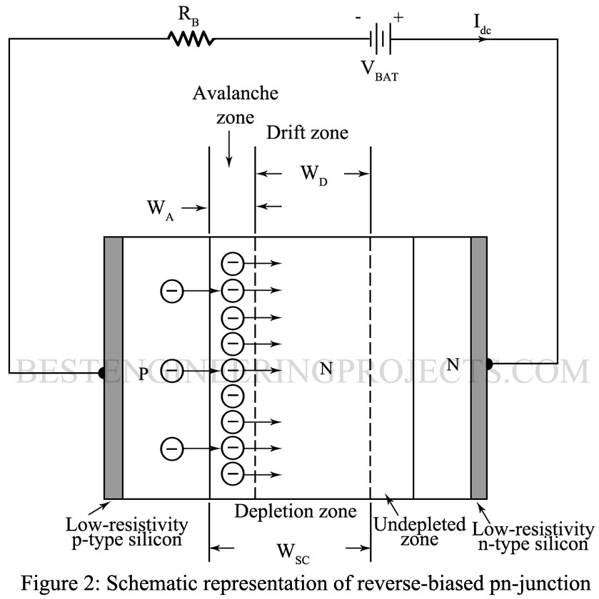
Figure 2 shows a schematic representation of an IMPATT diode reverse-biased into avalanche breakdown. As in any reversed-biased pn junction, a depletion zone forms in the n-type region of the diode; its width depends on the applied reverse voltage. The depletion zone acts as a nonlinear capacitor if Vdc is less than Vb. This property is utilized in varactor diodes. the saturation current, which flows while the reverse voltage is less than Vb, is usually on the order of 10 to 100 nA and is depicted in Figure 2 by a small number of electrons following to the right from the p+ region into the avalanche zone.
When Vdc is more negative than Vb, the small number of electrons comprising the saturation current have a very high probability of creating additional electrons and holes in the avalanche zone by the process of avalanche multiplication. The additional electrons are shown in figure 2 flowing from the avalanche zone into the drift zone. In this condition, a large current can flow in the reverse direction with little increase in applied voltage. This is the avalanche breakdown current, depicted in figure 1. The typical dc operating voltage across a diode will be between 70 and 100 V, depending on the diode type, temperature, and the value of the bias current, Idc. Typical avalanche breakdown currents (usually called the bias current) range from 20 to 150 mA.
Microwave Properties of the IMPATT Diode:
Let us assume that somehow a RG voltage, in addition to the dc breakdown voltage, exists across the depletion region of the IMPATT diode. This voltage can be expressed mathematically as
 …..(Eq.1)
This form of voltage is illustrated in figure 3 and would exist in practice in the common case where the diode is operated in a singly resonant circuit with Q greater than 10 or so. Under certain conditions the RF portion of this voltage induced a RF current that is more than 900 out of phase with the voltage, and therefore the diode has negative resistance. The argument leading to this conclusion are conveniently divided into two steps:
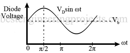
Figure 3: Voltage across the IMPATT diode depletion layer during oscillation
- First, as the voltage rises above the dc breakdown voltage during the positive half-cycle of the RF voltage, excess charge builds up in the avalanche region, slowly at first, and reaches a sharply peaked maximum at
 , that is, in the middle of the RF voltage cycle when the RF voltage is zero. This is shown in figure 4. Thus, the charge generation waveform , in addition to being vary sharply peaked, lags the RF voltage by 900. This behavior arises because of the highly nonlinear nature of the avalanche generation process.
 - The second step in the analysis is to consider the behavior of the generated charge subsequent to . The direction of the field is such that, referring to figure 2, the electron drift to the right. The equal number of generated holes move to the left, back into the p+ contact, and are not considered further in this simple model.
 , that is, in the middle of the RF voltage cycle when the RF voltage is zero. This is shown in figure 4. Thus, the charge generation waveform , in addition to being vary sharply peaked, lags the RF voltage by 900. This behavior arises because of the highly nonlinear nature of the avalanche generation process.
 . The direction of the field is such that, referring to figure 2, the electron drift to the right. The equal number of generated holes move to the left, back into the p+ contact, and are not considered further in this simple model.
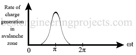 Figure 4: rate of change generation in the avalanche zone
The electrons drift at constant (saturated) velocity, vsat, across the drift zone. The time, t, they take to traverse the drift zone is simply the width of the drift zone divided by the constant velocity of the electrons:
 …..(Eq.2)
While the electrons are drifting through the diode, they include a current in the external circuit, as shown in figure 5. The current is approximately a square wave. By examining figure 3 and 5, it can now be seen that the combined delay of the avalanche process and the finite transit time across the drift zone has caused positive current to flow in the external circuit while the diode’s RF voltage is going through its negative half-cycle. The diode is thus delivering RF energy to the external circuit or, in circuit terms, is exhibiting negative resistance. Maximum negative resistance is obtained when
 …..(Eq.3)
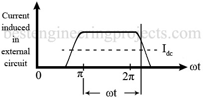
Figure 5: Current induced in the external circuit by the avalanche-generated charge drifting across the drift zone.
The term  is called the transit angle; IMPATT diodes are normally designed so that Eq. (3) is satisfied at or near the center of the desired operating frequency range.
IMPATT diodes are finding wide application in microwave oscillator and amplification scheme. They can produce 20-W continuous output at 10 GHz and are useful up to 300 GHz. While many two-terminal microwave devices exhibiting negative resistance have been developed in recent years, it appears that the Gunn diode (bulk-effect device) and IMPATT diode (true diode) have the most promising future. Among the other devices that have been utilized are the following:
- TRAPATT diode: It is similar to the IMPATT diode.
- Baritt diode: It has two junctions separated by a transit time region.
- Tunnel diode: Its use as a microwave power source/amplifier has diminished as Gunn devices and IMPATTs have become readily available.