a boat in tempest-tossed seas? That’s approximately what Frequency Shift Keying (FSK) accomplishes—it’s a method of data transmission through frequency alternating on and off, like Morse code in the ether but infinitely, infinitely faster.
How FSK Generation Works
One way to generate FSK is by tweaking the capacitor in an oscillator’s tank circuit. When the transmitter is keyed, the capacitor kicks in, changing the frequency. In narrowband FSK, instead of fiddling with capacitors, you can shunt capacitance across a crystal and let frequency multipliers do the heavy lifting.
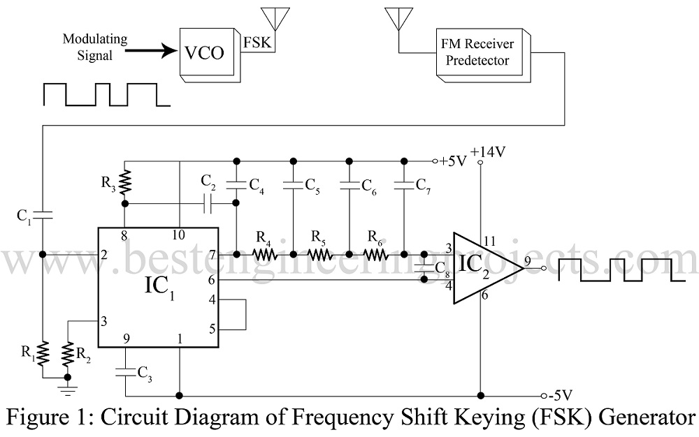
Another way? Use a voltage-controlled oscillator (VCO). It’s like having a tiny musical instrument that changes pitch depending on the input voltage. The circuit (see Figure 1) does exactly this, taking a rectangular modulating signal and feeding it into a PLL 565-based VCO. The output? A clean, modulated FSK signal, ready for transmission.
The Receiver and Signal Detection
A standard FM receiver picks up the FSK signal, passing it through intermediate frequency (IF) amplifiers. At this point, the magic begins: a 565 PLL (IC1) locks onto the input frequency, tracking its shifts between two points. The output at pin 7? A smooth DC shift that mirrors the original modulating signal.
To clean things up, we use a loop filter capacitor (C4) to adjust overshoot and a three-stage ladder filter to strip out unwanted frequencies. But hold on—the PLL output is a bit too rounded for logic circuits. That’s where IC2 (710 comparator) steps in, sharpening the edges and making the output crisp and binary-friendly. The final FSK signal emerges from pin 9 of IC2, ready to roll.
Why It’s Cool
- Reliable Data Transmission – FSK is immune to amplitude noise, making it perfect for radio comms.
- Smooth Signal Processing – The PLL cleans up the shifts, ensuring precise data recovery.
- Simple Yet Effective – A few well-chosen components make this circuit rock-solid.
Parts List for FSK Generator Using PLL 565
Resistors (all ¼-watt, ±5% Carbon)
- R1, R2 = 600 Ω
- R3 = 1 KΩ
- R4 – R6 = 10 KΩ
Capacitors
- C1 = 0.1 µF (Ceramic Disc)
- C2 = 0.001 µF (Ceramic Disc)
- C3 = 0.05 µF (Ceramic Disc)
- C4 – C7 = 0.2 µF (Ceramic Disc)
Semiconductors
- IC1 = 565 (General-purpose PLL IC)
- IC2 = 710 (BiCMOS op-amp with CMOS input stage)
Wrapping It Up
So, next time you send a text or talk over a digital radio, remember: behind that crystal-clear communication is an FSK generator quietly flipping frequencies like a pro. Whether it’s old-school modems or modern wireless systems, FSK remains one of the simplest, most effective ways to send data.
