Different gadgets have been introduced to meet our requirements ranging from basic needs to classy needs of humans. With this development in recent years, day by day people has grown more sophisticated. Putting human comfort as a main concern, hereby we have presented a circuit to remotely control several electrical or electronic gadgets connected to it. The unique feature of the circuit DTMF-based remote control system in comparison to other remote control systems like IR remote control is that this circuit employs FM transmission and reception, for this reason, it can be used for a comparatively longer range of control systems.
Using DTMF based remote control circuit we can control (switch on/off) any type of device by keying the number allocated to it. Since the keyboard used with the transmitter is similar to those used in the basic version of DTMF telephones, the circuit implementation becomes easier. The entire DTMF-based remote control system is composed of two subsystems which are described briefly in the paragraphs given below.
Circuit Description of DTMF Based Remote Control System
Code generator and transmitter
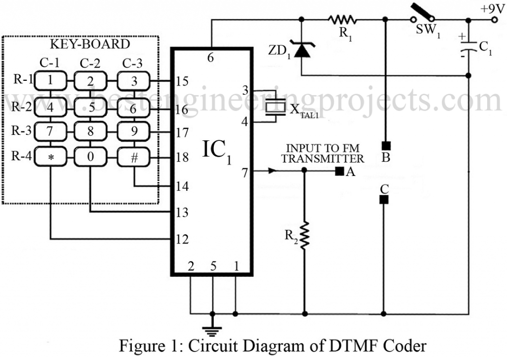
This part of DTMF based remote control system produces the code for control and transmits it to the respective gadget requesting operation as designed FIG.1 gives a clear view of the code generator part. It is a standard DTMF generator built around IC1 (UM91215B). IC1 generates the DTMF signal in correspondence to the number entered from the keyboard. The generated signal is then fed to an FM transmitter. Large numbers of FM transmitter circuits are available online, we can make use of any of them. Therefore for the simplicity of the entire circuit, the part of the transmitter is not included here. One must not forget that the operating range of the system depends on the range of the transmitter used.
Receiver and decoder
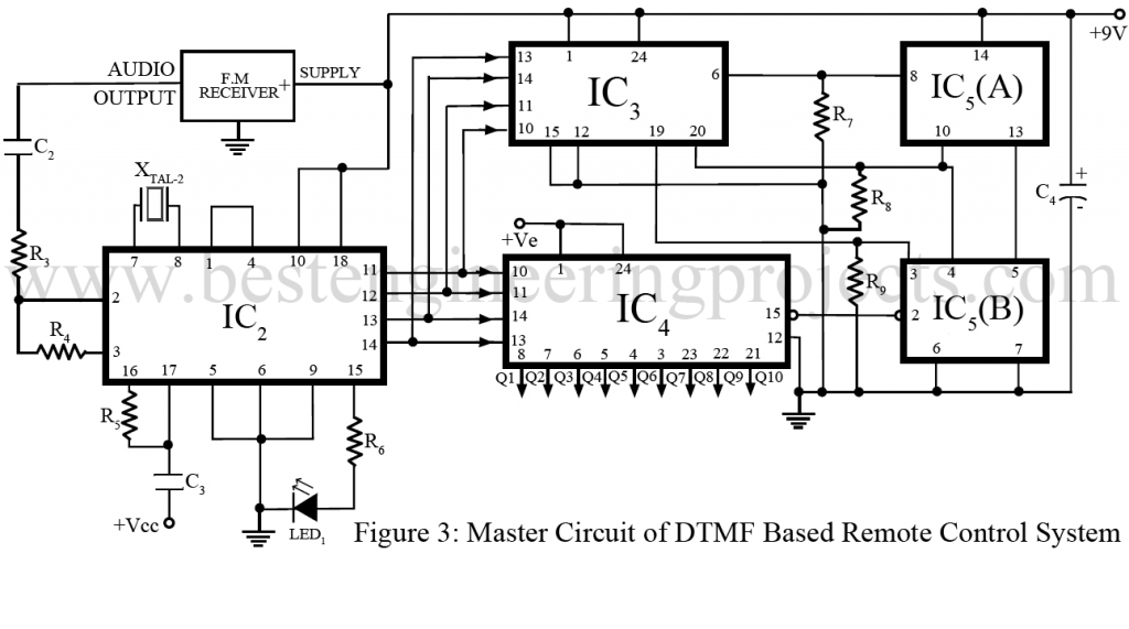
Fig. 3 gives the schematic diagram of the receiver and decoder for the DTMF-based remote control system which is here refer as a master circuit. Here again, a common FM receiver kit replaces the receiver portion which is easily available in the market. The output of the FM receiver is a carbon copy of the DTMF signal keyed in at the remote transmitter end. This output of the FM receiver is then fed to DTMF decoder IC2 (CM8870P) which gives a binary number as an output corresponding to the signal received from the transmitter.
Thus obtained -bit binary output is fed to IC3 (CD4067), which is a -line to 16-line decoder IC. One of the outputs of IC3 will go high, depending on the binary input fed in. IC3 produces a predetermined sequential output that activates IC4 (CD4067) via two flip-flops IC5 (a) and IC5 (b) connected to its output terminal. Two extra outputs of IC3 are used for activating/deactivating IC4. Similarly, the outputs from IC4 are used to switch the state of toggle flip-flops, which in turn control the devices using suitable interface (relay driver optocoupler, etc.) circuits.
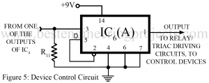
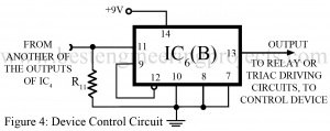
In Fig.4 and fig.5, we can observe two toggle flip-flops wiring using IC6 (CD4013). IC6 circuit should be repeated for other pairs of outputs of IC4. The circuit we have presented here can control up to 10 devices using outputs of IC4.
Operation of the Circuit DTMF based Remote Control System
The entire circuit of DTMF based remote control system bears the ability to control 100 different gadgets (switch on and switch off). To understand the control mechanism, we can assume all the 100 channels are grouped in a 10×10 matrix format. That means, there are 10 locations, with each location having 10 outputs to control up to 10 gadgets connected to it.
For clear understanding, let’s go with an example if we want to switch on a gadget numbered 5 at location 3. For this operation, the particular numbers to be entered in the sequence are; 3 # 5 *, in that order. The buttons marked # and *, generally available on all the keyboards, are used to activate and then deactivate a particular location.
As we receive the binary code for decimal number 3, pin 6 of IC3 of the decoder circuit goes high, making the set input (pin 8) of IC5(a) high. This causes pin 13 of this flip-flop to go high, thereby making pin 5 (data input) of IC 5 (b) also high. Then on receiving the next digit #(corresponding to decimal digit 12), the D flip-flop configured around IC5 (b) is clocked with the help of pin 19 of IC3 and in turn, IC5 (b) is activated and its output at pin 2 enables IC4 by taking its pin 15 active low.
The next key is digit 5 will make the corresponding output of IC4 (pin 4) go high. This positive-going pulse can then be used to trigger IC6 (CD4013) configured as a toggle flip-flop. In the circuit, the gadget to be controlled is connected to the flip-flop via relay driver, optocoupler, etc, as required. Receipt of the next input * (corresponding to decimal digit 11) will then make pin 20 of IC3 high to reset IC4 and hence disable IC4. However, this will not change the state of the gadget under control. Thus whenever the * button on the keypad is pressed (transmitted), all the locations get reset/deactivated but the existing latched state of the devices (“on or off”) at all the locations remains unaffected.
To switch on gadgets at other locations the numbers on the keypad should be pressed (transmitted) as per the sequence mentioned earlier. Now to switch off the gadget, the above switching process, i.e. transmits 3 # 5 * for switching off (in fact, toggling the existing state) device/gadget 5 at location 3, must be repeated. The sequence should be strictly followed, otherwise, false switching may occur and the control mechanism fails. The schematic diagram in Fig. 3 shows the wiring for location 3.
The circuit in Fig. 3 needs to be repeated for each location with only a slight change in the output pin of IC3, which is to be connected to ‘set’ pin 8 of IC5 (a). For locations 1 through 10, IC3 pins 8, 7, 6, 5, 4, 3, 23, 22, and 21 respectively should be connected to pin 8 of IC5 (a). For two units located near each other, a common FM receiver may be used.
One must remember that the binary equivalent code for “0” in the keypad equals decimal “10”. To avoid confusion, we can assume “0” on the keypad as “1”. For the same reason, (pin 9) output of IC3 and IC4 should never be used; instead, pin 21 representing location/device 10 may be used.
Construction and Testing of DTMF Based Remote Control System
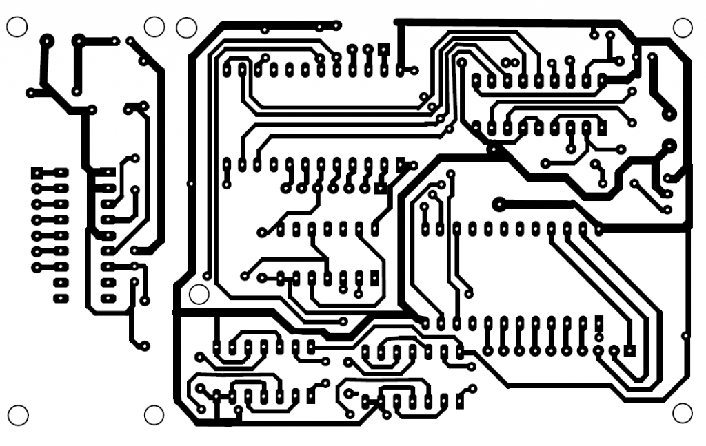
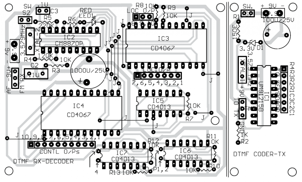
The circuit can be built on a Veroboard. However, an actual-size, single-sided PCB comprising circuits in Figs 1 and 3, except the FM transmitter and receiver modules, is shown in Fig.6. The component layout is shown in Fig.7. The circuit of IC6 has been repeated on the PCB to enable control of up to 4 devices.
Fig: 6 Solder Side PCB Design
Fig: 7 Components Side PCB design
The DTMF generator and FM transmitter should be housed in a metal box with the keyboard suitably placed. Be careful to watch the supply voltage of the FM receiver module if it shares a common supply with the system. After finishing the construction, switch on the transmitter and connect a small speaker or amplifier to the output of the FM receiver. Then press any key on the keyboard and at the same time tune the FM receiver until a clear tone is heard and the signal received LED starts glowing. Always tune the FM receiver where there is no signal from any radio center. If the output of the FM receiver is too low, a low-power, the compact amplifier may have to be used between the receiver and decoder. The system is now ready for use.
Check out other remote controller circuits posted on bestengineeringprojects.com
- IR Remote Controller Fan Regulator using AT89C2051
- Load Protector Circuit and Remote Switching
- Infrared Remote Controller Using Arduino
- Universal Arduino IR Receiver Circuit
PARTS LIST OF DTMF BASED REMOTE CONTROL SYSTEM
|
Resistors (all ¼ W, ± 5% carbon, unless stated otherwise): |
|
R1 = 150 Ω R2, R6 = 1 KΩ R3, R7 – R11 = 10 KΩ R4 = 120 KΩ R5 = 220 KΩ |
| Capacitors |
| C1 = 100uF, 25V (electrolytic capacitor)
C2, C3 = 0.1uF, (ceramic disc) C4 = 1000uF, 25V (electrolytic capacitor) |
| Semiconductors |
| IC1 = UM91215B DTMF dailer
IC2 = CM8870P DTMF decoder IC3, IC4 = CD4067 Demultiplexer IC5, IC6 = CD4013 Dual D Flip-Flap ZD1 – 3.3V, zener diode LED1 – 5mm Red LED |
| Miscellaneous |
| SW1 – On/Off switch
– Keyboard Xtal-1, Xtal-2 = 3.579542 MHz crystal – +9V DC power supply or battery – TRANSMITTER Antenna |
HI KRISHAN I M A CLG FINAL YEAR STUDENT WANNA HELP…..
WE HAVE TO DO A ELECTRONICS PROJECT EVERY YEAR AND UNFORTUNA TLY I GOT THIS PROJECT SO WILL U PLZ HELP ME
KOII DIKKT NHI H BNANE ME BUT PROJECT CHLNA BHT JRURI H SO KUCH HELP KER SKTE HO PLZ…
IF YES PLZ SEND ME FRIEND REQUEST ON MY FACEBOOK ID I SERCHED YOU BUT TUM MILE NHI SOO PLZ
ITS PANCHI.MISHRA.927
THANKS HOPE U HELP
APPiiii…
:)