In this article, we are satisfying the curiosity of electronics hobbyists, you and I alike by making a calling bell circuit diagram. The project can be set up in different rooms of an office or hospital and the attendant or office boy waiting place or nursing station. When a call is made from any of the rooms the attendant can be notified through the bell and he/she can verify the room from which the call is made by looking at the display showing the room number. Thus this project allows Nine different users from their respective rooms or beds to call an attendant or an office boy or a nurse.
This project is built around four different ICs. Let us look at them briefly so that we can understand the whole Calling Bell Circuit Diagram thoroughly.
10-Line-To-4-Line Priority Encoder (74LS147): Priority encoder converts a maximum of 2n input lines to the n outputs and 74LS147 priority encoder converts 10 input lines to 4 BCD (Binary Coded Decimal) output lines. The 74LS147 provides priority decoding of the inputs to ensure that only the highest-order data line is encoded. The Functional table (Truth Table) is shown below:
Functional Table (Truth Table)
|
1 2 3 4 5 6 7 8 9 10 11 12 |
Inputs Outputs 1 2 3 4 5 6 7 8 9 A B C D H H H H H H H H H H H H H X X X X X X X X L L H H L X X X X X X X L H L H H H X X X X X X L H H H L L L X X X X X L H H H H L L H X X X X L H H H H H L H L X X X L H H H H H H L H H X X L H H H H H H H H L L X L H H H H H H H H H L H L H H H H H H H H H H H L |
| Inputs | Outputs | |||||||||||
| 1 | 2 | 3 | 4 | 5 | 6 | 7 | 8 | 9 | A | B | C | D |
| H | H | H | H | H | H | H | H | H | H | H | H | H |
| X | X | X | X | X | X | X | X | L | L | H | H | L |
| X | X | X | X | X | X | X | L | H | L | H | H | H |
| X | X | X | X | X | X | L | H | H | H | L | L | L |
| X | X | X | X | X | L | H | H | H | H | L | L | H |
| X | X | X | X | L | H | H | H | H | H | L | H | L |
| X | X | X | L | H | H | H | H | H | H | L | H | H |
| X | X | L | H | H | H | H | H | H | H | H | L | L |
| X | L | H | H | H | H | H | H | H | H | H | L | H |
| L | H | H | H | H | H | H | H | H | H | H | H | L |
(H = HIGH Logic Level, L = LOW Logic Level, X = Irrelevant)
Check out the article on Decoder and Encoder IC
Hex Inverter (74LS04): Hex inverter performs the inverting operation i.e. high logic level to low logic level and vice-versa. 74LS04 is an inverting IC consisting of six not gates and its Functional table are shown in the figure below:
Functional Table (Truth Table)
| Inputs (A) | Outputs (Y = A) |
| H | L |
| L | H |
(H = HIGH Logic Level, L = LOW Logic Level)
Check out the article on Hex Inverter IC
7-Segment Decoder Driver (74LS247): The decoder function is exactly the opposite of the encoder i.e the n BCD inputs are converted to the maximum of 2n output lines. 74LS247 is an active low output decoder used to convert 4 BCD input lines to 7 output lines and these output lines correspond to the 7 (a-g) segment of the 7-segment display. The simplified Functional table (Truth Table) is shown below:
Functional Table (Truth Table)
| Inputs | Outputs | Corresponding
Decimal Number |
|||||||||||
| A | B | C | D | a | b | c | d | e | f | g | |||
| L | L | L | L | H | H | H | H | H | H | L | 0 | ||
| H | L | L | L | L | H | H | L | L | L | L | 1 | ||
| L | H | L | L | H | H | L | H | H | L | H | 2 | ||
| H | H | L | L | H | H | H | H | L | L | H | 3 | ||
| L | L | H | L | L | H | H | L | L | H | H | 4 | ||
| H | L | H | L | H | L | H | H | L | H | H | 5 | ||
| L | H | H | L | H | L | H | H | H | H | H | 6 | ||
| H | H | H | L | H | H | H | L | L | L | L | 7 | ||
| L | L | L | H | H | H | H | H | H | H | H | 8 | ||
| H | L | L | H | H | H | H | H | L | H | H | 9 | ||
(H = HIGH Logic Level, L = LOW Logic Level, Note: refer to datasheet for full functional table)
Check out the article on BCD to 7 Segment Display Driver
555 Timer IC: 555 timer IC is one of the most popular ICs in the field of electronics as it is used in a variety of timer, delay, pulse generation, and oscillator applications. 555 IC can be operated in two modes: monostable operation and astable operation.
In Monostable operation, output pulse duration is determined by the combination resistor RA and capacitor C and is given by t = 1.1RA C.
Components Required for Calling Bell Circuit Diagram
| Resistor (all ¼-watt, ± 1% Carbon Unless Stated Otherwise) |
| R1-R9, R12, R16, R17 = 1kΩ
R10, R13-R15 = 10kΩ R11 =2.2kΩ |
| Capacitors |
| C1 =10000μF at 35V (Electrolytic Capacitor)
C2 = 0.1μF (Ceramic Capacitors) C3 = 0.01μF (Ceramic Capacitors) C4 = 220μF at 35V (Electrolytic Capacitor) C5 = 0.1μF (Ceramic Capacitors) |
| Diodes |
| D1 – D4 = 1N4148 (Switching signal diode) |
| Transistors |
| T1, T2 = BC547 NPN transistor (General Purpose Switching Transistor) |
| Voltage Regulators |
| U1 = LM7805 (5V voltage regulator) |
| Semiconductors |
| U2 = 74LS147 (10-Line-To-4-Line Priority Encoder)
U3 = 74LS04 (Hex Inverter) U4 = 74LS247 (7-Segment Decoder Driver) U5 = NE555 (Timer IC) BR1 = Bridge Rectifier |
| Miscellaneous |
| DIS1 = 7-Segment display (Common anode type)
LED1 – LED9 = any color LED S1 – S10 = On/Off Switch PZ1 = Piezo buffer (9V) TR1 = 220V AC to 12V-0V, 500mA step down transformer |
Circuit Diagram of Calling Bell Circuit Diagram
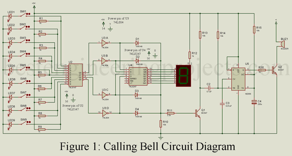
The above figure represents the exact circuit diagram.
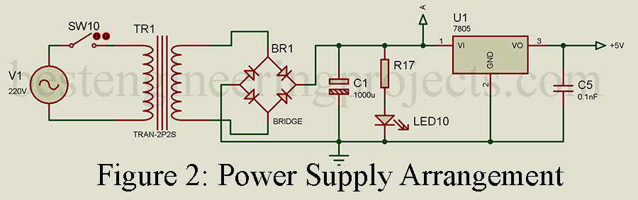
The 7805 voltage regulator provides a 5V regulated supply to the whole system, with the exception of the piezo buffer (bell), which is directly connected to a DC output from power supply made from transformer TR1 and rectifier.
Along with a combination circuit of an LED and a switch, the output pin of the 7805 voltage regulator (5V power supply) is connected to the input of the 74LS147 priority encoder. The inputs of the 74LS04 hex inverter are connected to the encoder’s output lines. Only 4 of the 6 NOT gates are used in the hex inverter, and their outputs are routed into the 4 inputs of the 74LS247 IC (7-Segment Decoder Driver). The 74LS247 7-Segment Decoder Driver IC is connected to the common anode type 7-segment display exactly as depicted in the diagram.
Through signal diodes D1 through D4 and a transistor T1, the timer IC 555 is connected to the output lines of the hex inverter 74LS04. Switching transistor T2 connects the 555 IC’s output to the piezo buffer. The 555 IC serves as a pulse generator in this application and is operated in monostable mode.
Circuit Working Principle:
Nine different officers will be able to call the attendant from their respective rooms with the flick of a switch when switch S10 (Power supply switch) is turned on.
Initial condition when no switch is pressed:
When switches S1 through S9 are opened, each of the inputs of the priority encoder will be high, and as a consequence, all of the encoder’s output lines will be high. As a result of the hex inverter’s conversion of high-level logic to low-level logic, all of the input lines of the 7-segment display driver will be low. In this situation, the 7-segment display driver IC will drive the display to show the correct room number, which will be displayed as zero, denoting that no calls are being placed from any of the rooms.
As the output of the hex inverter IC is low, diodes act as an open circuit as a result 555 timer IC will not be triggered.
When Switch S1 is closed:
When switch S1 is closed, LED1 lights up, and the current passes via switch S1 to the ground. The priority encoder’s first input (E1) drops low since no current is flowing there. Other input lines won’t change because the connecting switches to them are still open. As a result, input E1 drops low while input E2 – E9 stays high. Priority encoder output changes in response to input line changes. These outputs are inverted using a hex inverter before being sent to the inputs of a 7-segment display driver. Now the corresponding room number will be shown on display thanks to the 7-segment display driver IC, in this case, number One will be shown on the screen to show that the call was made from room 1.
In this instance, just one of the four NOT gates used in the hex inverter will have a high output; all other gate’s outputs will be low. The 555 timer IC will be activated when the output line of the hex inverter is high since the linked diode acts as if there were a short circuit. A pulse is generated when the 555 integrated circuits (IC) are triggered, and when this pulse is passed to the piezo buffer by switching the transistor T2, a ringing sound is audible.
Only one switch S1–S9 should be pressed at a time for smooth operation; otherwise, the 7-segment display may display the inaccurate room number.
Similar to this, the 7-segment display will display the room number from which the switch is pressed. This operation is fully described in the functional table that follows.
| Priority
Encoder Inputs |
Hex Inverter | Display Driver Outputs | NumberDisplayed in 7 segment Display | |||||||||||||||||||||||
| Inputs | Outputs | |||||||||||||||||||||||||
| Encoder Outputs | Display driver Inputs | |||||||||||||||||||||||||
| 1 | 2 | 3 | 4 | 5 | 6 | 7 | 8 | 9 | A | B | C | D | A | B | C | D | a | b | c | d | e | f | g | |||
| H | H | H | H | H | H | H | H | H | H | H | H | H | L | L | L | L | H | H | H | H | H | H | L | 0 | ||
| L | H | H | H | H | H | H | H | H | L | H | H | H | H | L | L | L | L | H | H | L | L | L | L | 1 | ||
| H | L | H | H | H | H | H | H | H | H | L | H | H | L | H | L | L | H | H | L | H | H | L | H | 2 | ||
| H | H | L | H | H | H | H | H | H | L | L | H | H | H | H | L | L | H | H | H | H | L | L | H | 3 | ||
| H | H | H | L | H | H | H | H | H | H | H | L | H | L | L | H | L | L | H | H | L | L | H | H | 4 | ||
| H | H | H | H | L | H | H | H | H | L | H | L | H | H | L | H | L | H | L | H | H | L | H | H | 5 | ||
| H | H | H | H | H | L | H | H | H | H | L | L | H | L | H | H | L | H | L | H | H | H | H | H | 6 | ||
| H | H | H | H | H | H | L | H | H | L | L | L | H | H | H | H | L | H | H | H | L | L | L | L | 7 | ||
| H | H | H | H | H | H | H | L | H | H | H | H | L | L | L | L | H | H | H | H | H | H | H | H | 8 | ||
| H | H | H | H | H | H | H | H | L | L | H | H | L | H | L | L | H | H | H | H | H | L | H | H | 9 | ||
(H = HIGH Logic Level, L = LOW Logic Level)
Low inputs for a priority encoder in the functional table above indicate that the switch corresponding to it is pressed. Input 1 is low when switch S1 is pressed, input 2 is low when switch S2 is pressed, and so on.
In each case, the 555 timer IC is triggered whenever the output lines of the hex inverter become high. The duration of the pulses generated by the 555 IC, which is set up to operate in a monostable operation and function as a pulse generator, depends on the resistor R15 and the capacitor C4.
t = 1.1R13 C1 = 1.1 10103 22010-6 = 2.42sec
Thus, a ringing sound from the piezo buffer can be heard for 2.42 seconds.