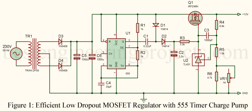
Efficient power regulation with a minimum drop in voltage has become quite necessary in modern electronics, especially when one works with low-voltage DC supplies. It is in meeting such requirements that a Low Dropout MOSFET Regulator becomes handy-assuring stable output with reduced dissipation of power. The following article elaborates on the design for an Efficient Low Dropout MOSFET Regulator, employing a 555 Timer Charge Pump to develop a higher gate voltage for the MOSFET, thereby realizing ultra-low dropout performance.
Why Use a Low Dropout MOSFET Regulator?
In conventional linear regulators, a significant amount of input voltage is dropped across the regulator, leading to inefficiencies, especially when working with low input voltages. A Low Dropout MOSFET Regulator overcomes this by using a MOSFET as the pass element, which requires only a minimal voltage difference between the input and output to regulate effectively.
For even better efficiency, we use a 555 Timer Charge Pump to boost the gate voltage of the MOSFET, enabling it to operate fully enhanced even at lower input voltages. This configuration minimizes the dropout voltage, making it ideal for applications that need stable regulation from a low DC input.
Key Components of the Low Dropout MOSFET Regulator Circuit
The following circuit main components are a Low Dropout MOSFET Regulator with a 555 Timer Charge Pump:
Resistors (all ¼-watt, ± 5% Carbon unless stated)
R1, R2 = 1 kΩ
R3 = 3.3 kΩ
R4 = 6.8 kΩ
R5 = 1.5 kΩ
R6 = 4.7 kΩ
VR1 = 1kΩ
Capacitor
C1 = 0.22 µF Ceramic
C2 = 3.3 µF/35V electrolytic
C3 = 1000 pF Ceramic
C4 = 33 pF Ceramic
C5, C6 = 1000 µF/35V electrolytic
Semiconductor
D1, D2 = 1N914
D3, D4 = 1N5408
U1 = 555 Timer IC
U2 = TL431
Q1 = IRFZ48
Miscellaneous
TR1 = 230V AC Primary to 12V – 0V – 12V, 2A Sec. Transformer
How the 555 Timer Charge Pump Works
In this Low Dropout MOSFET Regulator design, the 555 Timer is configured in an astable mode, producing a square wave output that powers the charge pump.
- 555 Output Low Phase: When the 555 output goes low, capacitor C2 charges through diode D1 to the input DC voltage.
- 555 Output High Phase: When the 555 output goes high, the stored charge in C2 boosts the voltage on C3 to nearly double the input voltage.
This boosted voltage is applied to the gate of the MOSFET (Q1), ensuring it is fully enhanced and can conduct with minimal resistance. By providing a higher gate voltage, the Low Dropout MOSFET Regulator maintains stable output with a very low input-output voltage differential.
Advantages of the Low Dropout MOSFET Regulator with 555 Timer Charge Pump
The use of the 555 Timer Charge Pump to provide a boosted gate drive voltage for the MOSFET has quite a number of desirable features:
- Ultra-Low Dropout Voltage: In this regulator, the dropout voltage is at its minimum because the fully enhanced MOSFET limits it; hence, it finds a suitable application in low-voltage DC applications.
- Improved Efficiency: Low RDS(on) of the MOSFET reduces the power loss, making this regulator highly efficient.
- Greater flexibility: with this arrangement, for instance, one of the big advantages of the configuration is that it can operate effectively with a lower input voltage for the battery-powered devices.
- Scalability for Higher Current: Parallel operation of several MOSFETs decreases the effective RDS(ON) further. This allows much higher currents to be passed by this Low Dropout MOSFET Regulator with a minimal resultant voltage drop.
Applications of the Power Efficient Low Dropout MOSFET Regulator
This is the important field where the Efficient Low Dropout MOSFET Regulator can apply:
- Battery-operated: These devices are suitable for applications requiring a high power efficiency with low dropout voltage.
- Low Voltage Power Supplies: Provides stable output with minimum loss of power even from a low input voltage.
- Sensitive Electronics: Useful in circuits needing a stable and regulated supply, with a minimum of power dissipation.
Design Tips for Low Dropout MOSFET Regulator with 555 Timer Charge Pump
To get the most out of this Low Dropout MOSFET Regulator:
- Select Low RDS(on) MOSFETs: Using MOSFETs with a low drain-source resistance reduces the dropout voltage significantly.
- Use High-Quality Capacitors: Capacitors in the charge pump should be high quality and rated appropriately for the input voltage.
- Parallel MOSFETs Considerations: Applications needing higher current can parallel multiple MOSFETs, which decreases the effective RDS(ON), further reducing the dropout voltage and further improving thermal performance.
Conclusion
Following regulator is the most appropriate and efficient solution to get low dropout voltage from DC rail. The below regulator reduces the power losses by incorporating a 555 timer, which in turn enhances the gate voltage of the MOSFET hence providing stable output with minimum input voltage requirements. Ideal for power sensitive applications, it makes the project great for any electronic work using low voltage DC supplies.
For more details and an in-depth view of similar circuits, follow the Ultra-Low Dropout MOSFET Linear Regulator with Short Circuit Protection article.
