In this article you will learn about emitter efficiency, base transport factor, The early effect, dynamic emitter resistance and amplifier action of transistor.
What do you mean by amplifying action of transistor?
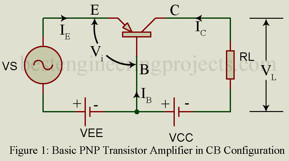
A transistor may serve various functions but basically it is used to amplify an electrical signal. Figure 1 gives the basic circuit of a PNP transistor amplifier in common base (CB) configuration. However, we may use an NPN transistor and get the same results.
In figure 1, the transistor is biased for active region operation i.e. JE is forward biased using voltage source VEE and JC is reverse biased using voltage source VCC. The emitter to base circuit forms the input side of the amplifier while the collector to base circuit forms the output side. The signal voltage VS to be amplified is applied at the input side. A load resistor RL is connected in the output circuit and the amplified output voltage is developed across RL.
The increment across RL is several times greater than the increment
providing the necessary voltage amplification. The ratio of output voltage increment
to the input voltage increment
is called the voltage gain or voltage amplification of the amplifier.
We may obtain an expression for the voltage gain of the CB amplifier of Figure 1. Thus, output voltage is given by,
……(1)
Where is the small signal current gain of CB transistor and is given by,
………(2)
But,
Hence, the voltage gain AV is given by,
………(3)
But is close to unity while RL can be kept much greater than re1 resulting in high voltage gain AV.
It is obvious that in effect the transistor acts to transfer current in the low resistance input circuit to high resistance output circuit. This action may be referred to a transfer resistor action from which the word transistor has originated.
Emitter Efficiency, Base Transport Factor and Transistor 
Emitter Efficiency The emitter efficiency or injection efficiency denoted by Greek later is defined as,
……..(4)
In a PNP transistor we have,
Thus, the emitter efficiency is the faction of the total emitter current which contributes to collector current. Hence, the emitter efficiency should be as large as possible. In order to maximize emitter efficiency, emitter region conductivity should be made much greater than the base region conductivity
. Typically, emitter efficiency is as large as 0.999 at low frequencies and 0.993 at high frequencies.
Base Transport Factor
It is defined as,
Base transport Factor
……….(5)
For pnp transistor,
……….(6)
Where IpC is the minority carrier hole current reaching JC (in a pnp transistor)
From equation 5 and 6 we get,
………(7)
The Early effect (Base Width Modulation) | Amplifying Action of Transistor
Consider a pnp transistor biased in the active region. Due to forward bias at JE, the depletion layer width at JE is negligible small. However, because of reverse bias at JC, the depletion layer is wide and it penetrates both in the base region and the collector region. But the doping of the base region is much smaller than that of the collector region. Hence, the penetration of the depletion layer at JC into the base region is much greater than the penetration into the collector region. The effective width of the base, therefore, gets reduced. As the magnitude of the reverse bias at JC increases, the effective base width W decreases. The phenomenon is known as the Early effect or base width modulation.
Effect of Base Width Modulation | Amplifying Action of Transistor
Decrease in the effective base width with the increase of magnitude of the reverse bias at JC produces the following three effects:
- Reduction in the chances of recombination of injected minority carrier holes (in a PNP transistor) in the base region resulting in increased base transport factor and hence increased
.
- Increased concentration gradient of minority carrier holes (in a PNP transistor) in the base region resulting in increased injected hole current IpE at JE.
- For extremely large value of reverse collector bias, the effective base width reduces to zero resulting in breakdown of the transistor action. This phenomenon is called punch-through. The value of the collector voltage at which punch through results is called the punch through
Dynamic Emitter Resistance | Amplifying Action of Transistor
The dynamic emitter resistance of a transistor indicated by re1 is defined as the reciprocal of the slope of the emitter current versus emitter voltage characteristic. Thus,
……..(8)
Obviously re1 is the same as the dynamic resistance of JE forming a pn diode and is, therefore, given by,
………..(9)
For Ge, whil for Si,
for rated forward current and
for large currents.
Thus, re1 varies inversely as the emitter current IE. At room temperature (300K) and with , Equation (9) yields,
Where re1 is in ohms and IE is in milli – amperes. Obviously re1 is always small.
