Monostable multivibrator generates square wave but it has only one stable state and another quasi-stable state. The circuit ordinarily stays in the stable state. On application of an external trigger signal, circuit changes state to quasi-stable state and remains in the quasi-stable state for a predetermined period of time and then reverts back to the stable state automatically. The time duration of the quasi-stable state is determined by the circuit components and parameters and is independent of the rate of occurrence of triggering pulse.
BJT monostable multivibrators may be of the following types:
- Self-biased monostable multivibrator
- Collector coupled dual power supply monostable multivibrator
- Single transistor monostable multivibrator
- Emitter coupled monostable multivibrators
We here consider only the self-biased BJT monostable multivibrator.
Self-Biased BJT Monostable Multivibrator
Fig 1 gives the basic circuit. In the normal stable state, transistor T2 is held in saturation by the timing resistor R while the transistor T1 is held in the OFF state by reverse biasing its emitter junction. To keep the transistor T1 OFF, the emitter voltage across the common resistor RE between the emitter and the ground should be greater than the base voltage of T1.

State I: Stable State Fig 2 gives the equivalent circuit in the stable state with T1 OFF and T2 ON. The following equations are valid for this state.
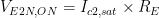
(A) Transistor T2 ON


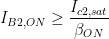
For large value of 

(B) Transistor T1 OFF: To keep the transistor T1 OFF, it is necessary that both the junctions be reserved biased. Collector junction is already reversed biased but to reversed bias the emitter junction we should have the base voltage of T1 less than the emitter voltage by 0.5 to 1.5 volt.
State II Quasi-Stable State: At the time instant t=0, a negative trigger pulse appears at the collector of T1. This negative trigger pulse is conveyed through the timing capacitor to the base B2 of T2 causing reduction in conduction of T2. This cause increase in collector current in T2 which increase is transferred through the resistive network R1 – R2 and speed up capacitor Cm1 to the base of T1. This tries to forward bias T1 and tries to bring T1 into conduction. Increased conduction in T1 causes lowering of the collector voltage of T1. This is cumulative process and this regenerative feedback force T1 into ON state and T2 into OFF state. Collector Rc1 is kept greater than Rc2 in order to have close-loop gain greater than unity (one) during the transfer of conduction.
In the quasi-stable state, during the time interval 0 < t < T, the timing capacitor C charges through the timing resistor R and the ON transistor T1 from the initial value VB2N,OFF towards supply voltage VCC. This charging process is exponential and has time-constant of RC. When VB2N reaches the value VB1N,ON, T2 starts conducting and again stable state established. The next cycle of similar operation occurs when next trigger pulse is applied. It may be shown that the periodic time T of the quasi-stable state is given by,
![T = RC ln [\dfrac{V_{CC}-V_{B2N,OFF}}{V_{CC}-V_{B2,ON}}]](https://s0.wp.com/latex.php?latex=+T+%3D+RC+ln+%5B%5Cdfrac%7BV_%7BCC%7D-V_%7BB2N%2COFF%7D%7D%7BV_%7BCC%7D-V_%7BB2%2CON%7D%7D%5D+&bg=ffffff&fg=000&s=0&c=20201002)