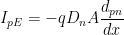
Figure 1 shows the various current components in a pnp transistor operating in the active region. The entire emitter current IE consist of two parts (i) hole current IpE carried by holes diffusing across JE from p-type emitter to n-type base and (ii) electron current InE carried by electrons diffusion across JE from n-type base to p-type emitter. The ratio 


Forward bias at JE results in injection of holes across JE into the base region. These minority holes diffuse through the base constituting the hole diffusion current IpE. This current is proportional to the slope of the hole density pn at KE. Hence this current IpE is given by,


Where Dp is the diffusion constant for holes and A is the cross-sectional area.
Similarly, InE is proportional to the electron density np at JE and is given by,
Where, Dn is the diffusion constant for electrons.
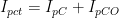
Total emitter current IE crossing JE is the sum of IpE and InE. Thus,

All these currents IE, IpE and InE are positive in a pnp transistor.
The holes while diffusion through n-type base region, meet majority carrier electrons ad some of these holes recombine with electrons giving rise to a small base current. The hole current Ipc on reaching the collector is, therefore, slightly less than IpE. The holes on reaching JC across it easily (since they travel down the potential barrier) and enter the p-type collector region. Since, the width of the base region is very small, almost all the holes injected into the base reach the collector junction and get collected by the p-type collector.
In addition to current IpC, there is another current at JC namely reverse saturation current ICO (or ICBO). This ICO is sum of two components: (i) current Inco caused by electrons diffused across JC from n-type collector to n-type base and (ii) current IPCO caused by holes diffusion across JC from n-type base to p-type collector. Hence, we have,

In equation 4, minus sign has been added to ICO intentionally so that IC and ICO may have the same assigned direction of flow.
IPCO results exclusively from the holes generated thermally within the base while Inco results from the electrons generated thermally within the collector.
Under the active region operation with JE forward biased, the collector current is given by,


Where 
In a pnp transistor, Ie is positive while both IC and ICO are negative since the current in the collector lead actually flows in the direction opposite to that indicated by the arrow on IC in figure 1.
Total diffusion hole current across JC from the base into the collector is,
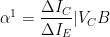
Large Signal Current Gain
The term

Term
DC Current gain 
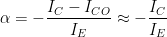
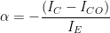
If ICO<IC then from equation 8, 
Thus, 
Quantity
Small Signal Current Gain 
It is defined as,
Where 

Increments 
Generalized Expression for Collector Current
Equation 6 giving IC in terms of ICO, 
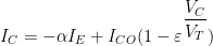
If VC is negative and large in magnitude compared to VT, Equation 11 reduce to equation 6.
Physical meaning of equation 11 is that the current in Jc (acting as a pn diode) gets supplemented by a fraction of IE coming from the emitter.
Example 1: In a PNP transistor in CB configuration, only 0.5% of the holes injected into the base through JE recombine with electrons in the base. If 

Solution:
Number of electrons combining with holes in the base region per 

Hence, the number of electrons entering the collector leads per 
Example 2: In a PNP transistor operating in the active region in CB configuration. The collector current equals 9mA and the emitter current equals 9.2mA. Calculate the value of
Solution:


Example 3: In a PNP CB Transistor operating in the active region, the emitter current IE = 8mA and 
Solution:
Hence,

Hence,

Example 4: In a PNP CB transistor operating in the active region, collector current IC = -5mA and the base current 
Solution:


Example 5: In a PNP CB transistor operating in the active region, the emitter current IE = 4mA, 

Solution:
Or,
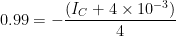
Where IC is in mA
Hence,

Hence,
![I_B = -[I_E + I_C] = -[4-3.964]mA = -36 \mu A](https://s0.wp.com/latex.php?latex=I_B+%3D+-%5BI_E+%2B+I_C%5D+%3D+-%5B4-3.964%5DmA+%3D+-36+%5Cmu+A&bg=ffffff&fg=000&s=0&c=20201002)