Common Source Amplifier
In this amplifier, input signal is applied between gate and source and the amplified output voltage is developed across a load resistor in the drain circuit. Thus, source is the common terminal between the input side and the output side.
Figure 1 gives the circuit of one stage of common source amplifier (CS) Amplifier using n-channel FET and with biasing arrangement. The typical component values are also shown in figure. This circuit is analogous to common emitter amplifier. On using p-channel FET, polarity of supply voltage is reversed. In the circuit of figure 1, Rs-Cs combination provides the self-bias.

Since no current passes through the reverse biased gate-source, the gate current IG is zero. Hence d.c. gate voltage is,
With d.c. drain current set to ID, the dc voltage at the source is,

The gate source voltage is then,

Or, 
However, quite often capacitor Cs is omitted from the circuit. Then resistor Rs no doubt provides the self-bias (caused by the flow of dc component of drain current) but also provides feedback from output circuit to the input circuit.
Analysis of Common Source Amplifier using FET
The analysis given below applies to both the n-channel and p-channel common source amplifiers. Figure 2 gives the ac equivalent circuit. Here FET has been replaced by its small signal model of figure 3.

On applying KVL to the output circuit we get

From equivalent circuit of figure 2,

On substituting the value of Vgs from equation (6) in equation (5) we get,

The output voltage Vo is developed across the load resistor Rd and is given by,

The minus sign associated with V0 as given by equation (8) shows that the output voltage V0 is 1800 out of phase with Vi.

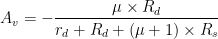
Hence voltage gain,
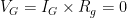
Since the gate current is zero, input resistance is,

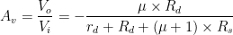
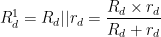
Making use of equation (8), figure 4 gives the equivalent circuit, called the Thevenin’s equivalent circuit, looking from load resistor Rd into the drain-to-ground N. Here (Thevenin’s) equivalent voltage is 

With Rs = 0 In case, Rs is bypassed by a high value capacitor CS i.e. if source S is effectively grounded, then in the above analysis, we may put RS = 0.
Then from equation (9),


Or, 
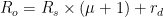
Where,
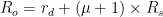
Output Impedance 
Numerical Problem on Common Source amplifier using FET
Example 1: A common source amplifier uses FET having dynamic resistance rd = 120 k-ohm and 
Solution:

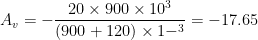
Voltage gain,

For Rd = 300 K-ohm,

For Rd = 600 K-ohm,

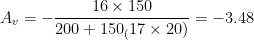
For Rd = 900 K-ohm,
Example 2: A common source amplifier uses loads resistance 


Solution:
Given that: 
Solution for (i) For 


Solution for (ii) For 


Solution for (iii) For